A deep-dive into Qualcomm's Hexagon NPU
I recently put together a rather elaborate presentation on my Computational Methods course, exploring Hexagon's inner workings and it is a marvel that I feel is worth writing about. Standard CPUs are great at unpredictable, branch-heavy control flow. But when you need to chew through massive arrays of fixed-point math (usually signal processing heavy stuff) running standard CPU instructions creates severe bottlenecks and is inefficient. Offloading this fixed-point arithmetic to an NPU architecture yields massive power savings.
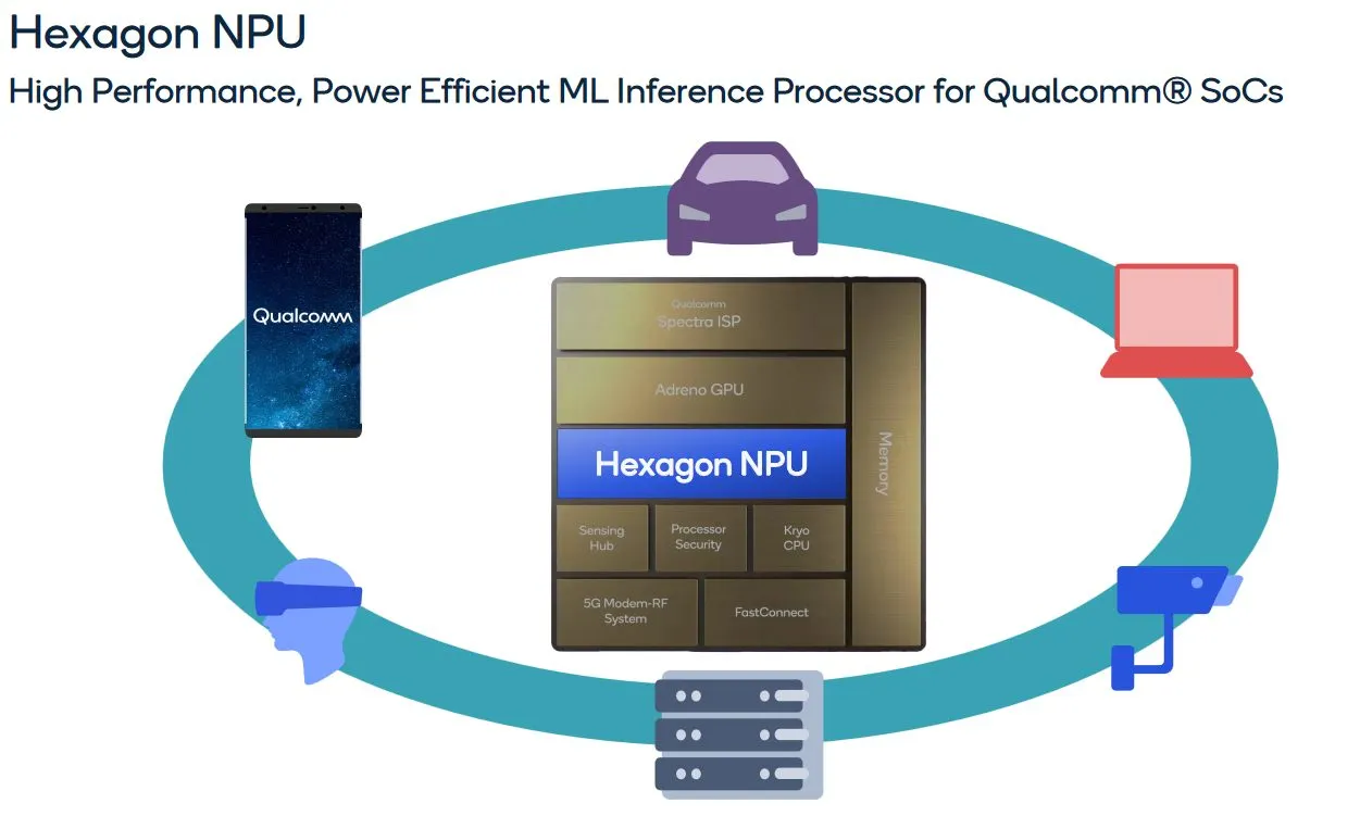
Hexagon used to be a Digital Signal Processor (DSP), but it has been rebranded as an NPU (Neural Processing Unit). We are going to dissect both its physical compute engines and its software programming model
Hexagon's Compute Engines
Introduced back in 2007, Hexagon was designed purely as a low-power scalar DSP for audio and voice encoding. Around 2018, as on-device machine learning exploded, Qualcomm started bolting dedicated AI accelerators onto their SoCs.
However, having discrete DSP and AI engines creates an architectural bottleneck: data movement, because we are bouncing intermediate tensors back and forth across external memory buses between separate hardware blocks, which is evidently wasteful.
In 2020, Qualcomm introduced a paradigm shift, fusing these previously isolated engines into a single unified architecture surrounding a very large shared memory pool.
The unified architecture consists of three differentiated compute cores:
- Scalar Core: The classic Very Long Instruction Word (VLIW) engine managing OS threads, control flow, and standard scalar arithmetic.
- Vector Engine (HVX): A massive SIMD powerhouse optimized for streaming parallel 1D arrays of signal and imaging data.
- Tensor Accelerator (HMX): Dedicated fixed-point matrix multiplication hardware purpose-built for deep neural networks.
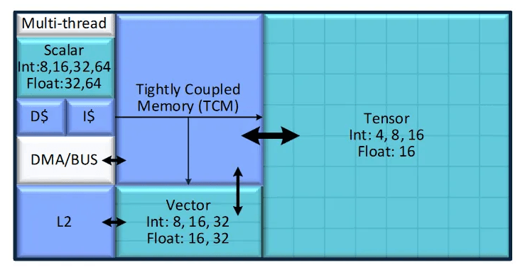
VLIW Scalar Core
Modern out-of-order ARM CPUs spend a big chunk of their silicon area and power on dynamic hazard detection, register renaming, and speculative branch prediction logic.
However, DSP architectures favor VLIW (Very Long Instruction Word) design. Instead of figuring out instruction dependencies on the fly, the compiler (hexagon-clang) does the heavy lifting statically at compile time, packing up to 4 instructions into a single execution packet fired simultaneously.
The execution pipeline is intentionally asymmetric:
- Slots 0 & 1: Primarily dedicated to memory operations (
Load/Store). - Slots 2 & 3: Primarily dedicated to arithmetic logic (
XTYPEmath) and branch jumping.
Slots 2 and 3 have specialized hardware registers like:
- Hardware Loop Registers (
lc0/lc1): These manage loop iterations natively in hardware. When a loop completes an iteration, the core decrements the loop counter and jumps automatically without executing explicit branch or decrement instructions. - Circular Buffer Registers (
CS0/CS1): Provide automatic modulo addressing. This is invaluable for algorithms like sliding-window FIR filters where pointer indices need to wrap around seamlessly.
Hardware Multi-Threading (SMT)
To hide memory fetch latencies without resorting to complex out-of-order execution logic, Hexagon relies heavily on Hardware Multi-Threading (SMT). A single shared Instruction Cache (I-Cache) feeds the execution pipeline, round-robin interleaving up to 6 hardware threads into the VLIW front-end on every clock cycle.
While threads share the fetch and math pipelines, every thread has its own physically dedicated Register File (RegFile). Because all register state is preserved on-chip simultaneously, context switching between hardware threads takes zero clock cycles.
There is no pushing or popping registers to stack memory.
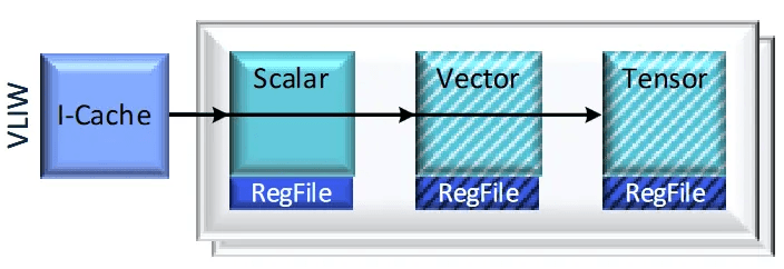
Powering up massive vector and tensor arithmetic blocks constantly would be grossly inefficient.
Therefore, Hexagon enforces an acquire/release resource model.
When a hardware thread boots up, it starts as a Scalar thread. To execute wide vector or matrix instructions, the thread must explicitly request coprocessor context (e.g., calling qurt_hvx_reserve() or qurt_hmx_reserve()). Once reserved, the physical SIMD or Tensor block wakes up and locks to that specific thread until released.
Memory Hierarchy
If a 1024-bit vector engine and a 16K MAC tensor unit pulled their working datasets through standard L1 cache, they would thrash the cache lines and evict all the scalar core's critical control flow state. To prevent compute engines from starving the control core as such, Hexagon segregates its memory access paths:
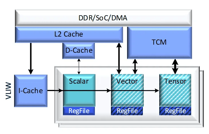
- L1 D-Cache: Strictly fenced off for the Scalar core.
- L2 Cache: The Vector engine bypasses L1 entirely, wiring high-bandwidth data paths directly into L2.
- TCM (Tightly Coupled Memory): A software-managed scratchpad SRAM, which has no hardware cache tags or lookup tables, guaranteeing deterministic, zero-miss latency. This does come with a trade-off, where the programmer must manually instruct background DMA engines to pre-fetch data tiles from external
DDRintoTCMahead of compute.
What makes the Hexagon go from a DSP to an NPU are the Hexagon Vector Extensions (HVX) and Hexagon Matrix Extensions (HMX). Let's learn more about these powerful units!
Hexagon Vector Extensions (HVX)
A standard ARM NEON SIMD register is 128 bits wide whereas a Hexagon HVX vector register (Vreg) holds 128 bytes (1024 bits) - eight times wider!
This allows a single instruction to operate on 64 half-word (16-bit) numbers simultaneously.
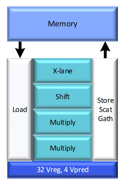
Because HVX is integrated into the VLIW packet scheduler, the core can dispatch up to four vector operations per cycle across specialized hardware blocks: two Multiply units, a fixed-point Shift scaling block, and an X-lane permutation unit for cross-lane data shuffling.
Furthermore, HVX natively supports vector Scatter/Gather. So, a single instruction can gather 128 discrete bytes from entirely non-contiguous memory addresses in TCM into a single vector register in one shot.
Hexagon Matrix Extensions (HMX)
While HVX crunches 1D vectors, HMX steps up to Tensors, allowing for the efficient acceleration of high-dimensional workloads, particularly inference of neural networks.
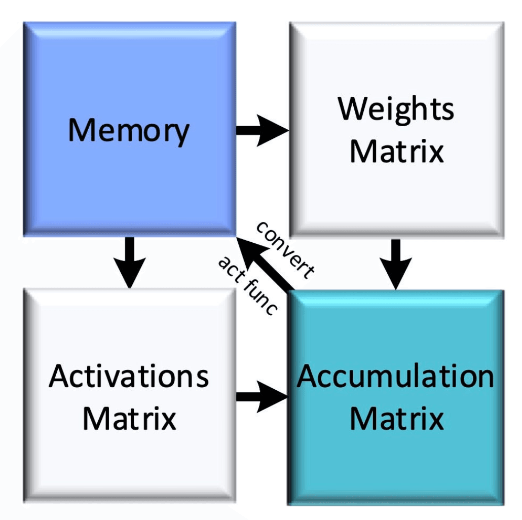
In a typical AI inference workload, HMX streams quantized Weights and Activations (supporting mixed integer bit-widths like FP16, INT8, or INT4) directly from memory into an Accumulation Matrix capable of performing up to 16,384 multiply-accumulate operations per clock cycle. Scaling and non-linear downconversions happen in dedicated hardware before writing final results back to memory.
Building for Hexagon
We now understand the architecture and capabilities of the Hexagon NPU. But that is only half the battle! How do we actually write code for such a specialized coprocessor? We certainly cannot just write code the same way we would for a standard ARM CPU!
Even though the main ARM CPU (e.g., Qualcomm Kryo) and the Hexagon DSP sit physically on the exact same silicon die, they exist in a state of strict architectural isolation:
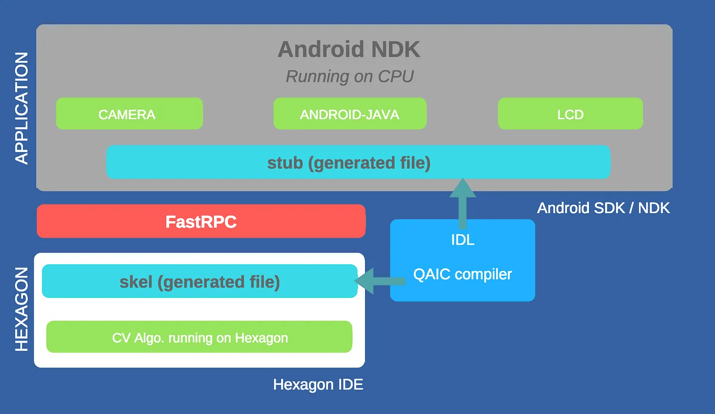
- Different Operating Systems: The ARM cores run a High-Level OS (Android or Linux), whereas Hexagon runs QuRT (Qualcomm Real-Time OS).
- Different Toolchains: ARM code is compiled via standard GCC/Clang, while DSP kernels require the specialized
hexagon-clangVLIW compiler. - Different Address Spaces: A virtual memory pointer allocated on the ARM CPU is not valid inside the Hexagon MMU.
Because of this disaggregation, an Android app or C++ daemon on the CPU cannot simply execute a function call across to the DSP, which leads us to learn the inter-processor communication protocols and standards of Hexagon.
Interface Definition Language (IDL)
To move data between the ARM CPU and the Hexagon DSP, both processors must agree on a rigorous contract dictating exactly what data moves across the bus and in which direction. We express this contract using an IDL (Interface Definition Language) file:
interface my_kernel : remote_handle64 {
   long compute(in sequence<long> input_data, rout long result);
};
Here, we have:
- Directional Qualifiers (
in,rout): Tell the RPC serializer how to handle memory buffers.inmeans the CPU serializes the array and sends it to the DSP.rout(remote out) signals that the ARM host pre-allocates an empty destination buffer, passes a reference across, and the DSP writes compute results directly into it. - Return Values: Methods strictly return a scalar
longorintstatus code (0for success, non-zero for system crashes). - Session Handles: Inheriting from
: remote_handle64equips every interface with an opaque 64-bit handle identifying the active DSP FastRPC session.
QAIC Compiler Workflow
When we build our project, the SDK's qaicidl compiler parses the single .idl file we created and automatically spits out three files:
my_kernel.h: This is a standard C header included by both host CPU and target DSP codebases.my_kernel_stub.c: This code is compiled into the ARM host application. It intercepts normal C function calls and serializes arguments into RPC packets.my_kernel_skel.c: This code is compiled into the DSP shared library (.so). It unpacks RPC packets arriving from the driver and invokes your actual DSP logic.

Implementing DSP Kernel Logic
With the contract generated, we write the actual computation logic in standard C on the Hexagon side:
#include "HAP_farf.h"
#include "my_kernel.h" // Auto-generated IDL contract

// 1. Session Initialization
int my_kernel_open(const char* uri, remote_handle64* h) {
    *h = (remote_handle64)malloc(1); // Assign stateless dummy session handle
    return 0; // 0 = Success
}

// 2. Session Teardown
int my_kernel_close(remote_handle64 h) {
    free((void*)h);
    return 0;
}

// 3. Core Compute Kernel
int my_kernel_compute(remote_handle64 h, const int* input_data,
                      int input_dataLen, int* result) {
    *result = 0;
    for (int i = 0; i < input_dataLen; ++i) {
        *result += input_data[i];
    }
    // Standard printf will fail on DSP. So we use the FARF macro to route logs via DIAG subsystem
    FARF(RUNTIME_HIGH, "DSP: compute successfully aggregated result %d", *result);
    return 0;
}
We can identify two important DSP idioms here:
- The IDL type
sequence<long>automatically translates into two C arguments: aconst int*pointer and an integerinput_dataLentracking array size. - Because Hexagon has no standard terminal stdout, calling
printf()crashes. We use theFARF()macro (Fast Asynchronous Remote Formatting) which routes logs through hardware DIAG FIFOs back to the ARM host terminal.
ARM host harness and FastRPC bridge
On the Android/Linux host side, we write a driver harness that spins up the DSP session and executes calls transparently over the FastRPC bridge:
#include "my_kernel.h"
#include "remote.h" // SDK FastRPC session control API

int main() {
    // 1. Configure a FastRPC Session to enable Unsigned PD (Protection Domain) on CDSP
    struct remote_rpc_control_unsigned_module data;
    data.domain = CDSP_DOMAIN_ID;
    data.enable = 1;
    remote_session_control(DSPRPC_CONTROL_UNSIGNED_MODULE, &data, sizeof(data));

    // 2. Open remote session handle pointing to compiled DSP skeleton library
    remote_handle64 handle = -1;
    my_kernel_open("file:///libmy_kernel_skel.so?_dom=cdsp", &handle);

    // 3. Execute transparent FastRPC calls
    int result = 0;
    int status = my_kernel_compute(handle, input_data, input_dataLen, &result);

    if (status != 0) {
        // Handle PDR (Protection Domain Restart) or SSR (Subsystem Restart) recovery here!
    }

    my_kernel_close(handle);
    return 0;
}
CDSP is the Qualcomm Hexagon DSP's Compute Domain, which is a special protection domain that allows unsigned user-space code to run on the DSP without requiring a full kernel driver.
It is the only way to run custom DSP kernels on Android without having to flash a custom kernel image. We have to explicitly enable it via remote_session_control() and inform that the DSP is running in an unsigned protection domain.
Zero-Copy ION Memory Allocation
By default, when you pass arrays into FastRPC, the driver physically copies the memory buffer from the ARM CPU heap into kernel space, shoots it over the bus, and copies it into the DSP heap.
If we are passing small config structs, copying is harmless. But in applications where we are streaming or processing megabyte-sized arrays or larger at very fast rates, that memory copy becomes a CPU bottleneck.
To bypass serialization copies, we allocate memory from the Android ION Heap via rpcmem_alloc().
ION memory occupies contiguous physical RAM pages wired directly to both processor MMUs. When FastRPC detects an ION buffer reference, it skips copying entirely and simply maps the physical page frames directly into the Hexagon DSP's virtual address space.

Simulator testing via hexagon-sim
Before flashing code onto real physical hardware like a DragonWing board, we can validate and benchmark our kernels locally on our workstation using hexagon-sim.
It is good to know that hexagon-sim is a cycle-accurate hardware simulator! It simulates the exact VLIW packet slots, instruction cache misses, and hardware thread interleaving cycles of the physical die.
# 1. Build DSP skeleton for target v68 architecture
make hexagon BUILD=ReleaseG DSP_ARCH=v68 NO_QURT_INC=1

# 2. Run compiled binary through cycle-accurate simulator
hexagon-sim \
  -mv68n_1024 \
  --simulated_returnval \
  --pmu_statsfile pmu_stats.txt \
  hexagon_ReleaseG_toolv19_v68/my_kernel_q
When the simulation completes, it dumps a pmu_stats.txt file containing exact hardware Performance Monitor Unit metrics—including total committed P-cycles (processor cycles) and instruction packet counts, allowing us to optimize inner loops down to the exact clock cycle.
References & Further Reading
- Joey, "Qualcomm's Hexagon AI Accelerators", The Chip Letter — Substack Article
- Qualcomm Architecture Documentation, "Hexagon Processors & NPU Overview" — Qualcomm Developer Portal
- M. Deore, "Hexagon DSP CPU Offload Architecture" — Medium Technical Deep Dive
- Qualcomm Hexagon DSP SDK Docs, "Introduction to Neural Processing Units" (80-77512-1)
- Qualcomm IQ-9 Series SoC Product Brief (Rev A, 87-83840-1)